

MSL FPGA INC ( Meishilong )plans to build a 2-5 nanometer wafer fab manufacturing project, consisting of MSL MEISHILONG Responsible for chip manufacturing in the future
MSL FPGA INC Specializing in programmable logic devices FPGA Research and Development, Design, and Manufacturing
MSL MEI SHI LONG Focused on research and development design FPGA Peripheral devices and production of various semiconductor devices and FPGA Supporting, with the continuous advancement of technology, MSL MEISHI LONG The products are constantly being updated and iterated, maintaining a leading position in the industry.
MSLFPGA The company plans to build a 2-5 nanometer wafer manufacturing project
A wafer fab is commonly referred to as a 'Fab',
1 「fabrication」( The abbreviation for manufacturing refers specifically to the production factory of integrated circuits (chips).
2. Foundry is closely related, which focuses on manufacturing rather than design
3. Provide production services for Fabless, a chip design company


 The chip factory park is mainly divided into two sections: energy supply (banquet hall) and manufacturing area. This time, we will mainly talk about its core manufacturing area, which includes: drawing wafer design, (chip front-end) wafer manufacturing, and finally packaging and testing. In the future, its daily task will be to do repetitive things to turn "silicon" materials into omnipotent chips. Silicon is the best material for manufacturing chips. Chip manufacturing involves carving circuit diagrams on semiconductors, as well as carving the beginning, so that it can produce binary "0" and "1". It can conduct electricity or not, and its conductivity can be changed by applying voltage, so it is referred to as a "semiconductor or integrated circuit (chip)".


 Research and development of wafer drawing design:
Firstly, design the wafer drawings in the office R&D center. First, draw the functional zones of the chip on the drawings. Then, design each zone and divide it into each node. Finally, import it into EDA Software continues to expand point by point design, using EDA Software can stack thousands of different circuits and simulate their real performance. Once the design is completed, the R&D center will send the design drawings to the core manufacturing area for production.

 Chip front-end (manufacturing) process:
Secondly, dust is not allowed to appear in the core (front-end) manufacturing production area, so the staff must clean their hands, wear dust caps, and then go to the changing room to wear special fixtures. These fixtures will block every part of the body to prevent the shedding of skin fat particles from polluting the inside. Before entering, they also need to go through a special shower room, where filtered air is sprayed out from dozens of nozzles to clean up the remaining dust on their bodies, and then officially enter the manufacturing area. There are more than 2000 equipment, including lithography machines, in the manufacturing area. The entire workshop is 1000 times cleaner than any operating room, and is equipped with advanced lithography machines from all over the world. For example, there is the Netherlands ASML delivered EUV Photolithography machine, using 13.5 nm Extreme ultraviolet light source, numerical aperture 0.55, supports 2 nm And more advanced manufacturing process nodes. The core part of chip manufacturing is the processing of silicon wafers, which first involves grinding and polishing the disc. From raw material purification, single crystal growth, ingot processing, slicing and chamfering, grinding and etching, polishing and cleaning, and more than ten other processes, the processing of silicon wafers is essentially the culmination of "extreme manufacturing" technology N The purity is controlled to atomic level surface smoothness, and each step directly affects the yield of the final chip. Then a layer of photoresist is coated on the surface of the silicon wafer, which is a material extremely sensitive to the ultraviolet light of the lithography machine. After coating with photoresist, it is put into the lithography machine. The lithography machine is somewhat similar to a photo printer, but its cost is over 200 million US dollars, and the printing accuracy is outrageous. The nozzle of the printing machine is equivalent to the size of a hair, while the lithography machine magnifies the hair by 10000 times and then carves a complex transistor on it. The ultraviolet light of the lithography machine is engraved by exposing it on the photoresist. This is the burst stage of the lithography machine, and extreme ultraviolet lithography (EUV) achieves 7 nm The following process, through 13.5 nm The wavelength lithography machine transfers the circuit pattern to the photoresist layer, and the etching accuracy needs to be less than 1.5 nm。 The steps of coating, exposure, and development need to be completed in a clean room to avoid nanoscale pollution. The ultraviolet lithography machine comes from the optical equipment above, which contains lenses and a mask containing circuit diagrams. Ultraviolet light projects the circuit diagram on the mask onto the silicon wafer for exposure. The exposed area solidifies and is preserved, while the unexposed area is "etched" away. Due to the need to build thousands of layers of circuits, these steps need to be repeated, with a total of more than 200 processes. The chip manufacturing area must purchase highly automated management to allow the machines to produce semiconductor chips, and then let the system manage these machines. The robot places the printed silicon wafer into a specially designed car, and then sends the car to the top track. The car quickly moves between each process along the track, and the moving car has sensors on it. Devices and chips, which can enable the entire system to recognize them, If the cars are too close to each other, they can also adjust the speed of movement. There are thousands of such track cars in the entire manufacturing area, and they need to connect more than 2000 machines, more than 160000 sensors, and over 800 million control points.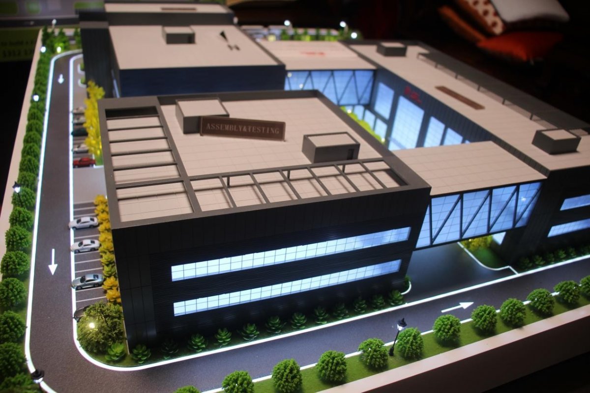
Finally, it enters the assembly and testing area, and most workers only need to remotely control the system. Thousands of processes are completed by automation. After completion, the trolley is removed to perform performance testing on the wafer, which is to test the silicon chips that are already close to the finished product. These silicon chips are the most complex integrated circuits in the world. After testing, these chips are cut out, and cutting and packaging are completed in the packaging area. The cutting method is not complicated, and the robotic arm has a cutting trajectory when walking under the program. Cut with a diamond blade, then extract the cut chip and place it on the integrated circuit board used for packaging the chip. That is the circuit board for communication between the chip and external devices. This is a thin wire made of gold, which is the best conductor. Welding with gold wire can maximize the performance of the semiconductor. Finally, packaging. Due to the sensitivity of silicon material to the environment, it must be sealed in a black protective disk. Throughout the packaging process, the final testing procedure is included. Qualified chips will be laser printed with silk screen labels, and finally packaged according to the order for the sales department to deliver to global customers. MSL FPGA INC We insist on making customers feel at ease and satisfied.


 MSL FPGA INC Plan to build a 2-5 nanometer crystal factory, consisting of MSL MEISHILONG Responsible for chip manufacturing
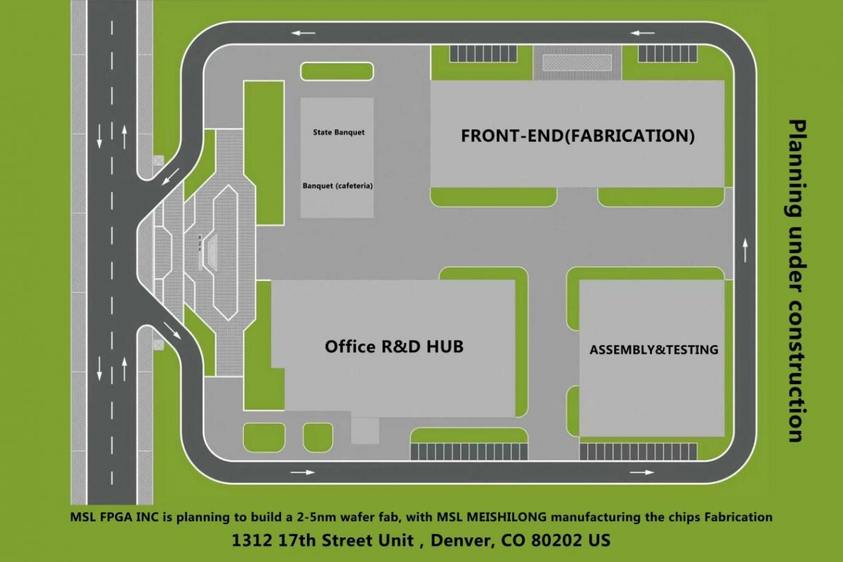
This is MSL FPGA INC We are planning to build a chip factory for 2-5 nanometer wafer manufacturing, located in MSL FPGA INC, 17th Street, Denver, Colorado 80202, USA.